
This is an excellent example of how unexpected properties can spontaneously arise in complex materials, a phenomenon scientists hope will be used to develop new technologies.
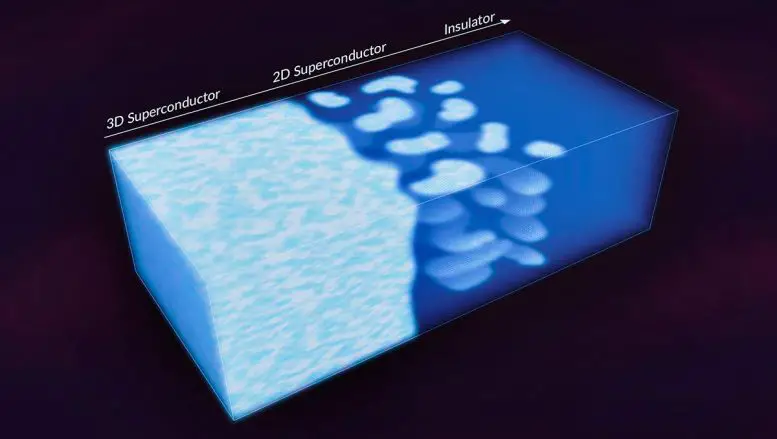
Creating a two-dimensional material with only a few atoms thickens takes work. This requires sophisticated equipment. Scientists were astonished to find 2D puddles in a 3-dimensional superconductor, which allows electrons to travel at 100% efficiency and with zero resistance.
The superconducting electrons in those puddles behaved like they were trapped inside a thin, sheet-like structure. This situation requires them to cross into another dimension where quantum physics rules differ.
Hari Manoharan (a Stanford University professor and researcher with the Stanford Institute for Materials and Energy Sciences at the Department of Energy’s SLAC National Accelerator Laboratory), who led the research, said, “This is a tantalizing instance of emergent behavior, which can often be difficult or impossible to reproduce by trying to engineer them from scratch.”
He said that it was as if the 3D electrons could choose to live in a 2D environment if they were given superconducting power.
This new phenomenon is called “inter-dimensional Superconductivity” by the research team. They reported it in the Proceedings of the National Academy of Sciences on April 12, 2021.
“What we discovered was a system in which electrons behaved in unexpected ways. “That’s the beauty and wonder of physics,” Carolina Parra, a postdoctoral researcher from SLAC/Stanford at the time of the study, said. She was responsible for the experiments that led to the visualization of the intriguing result. “We were extremely fortunate to find this behavior.”
Strange behavior of electrons
Superconductivity was first discovered over a century ago. However, its utility was limited because materials can only become superconducting at temperatures close enough to those found in deep space.
The 1986 announcement that scientists had discovered a new superconducting material sparked a wave of research. This includes developing new versions of the materials and finding new ways to make them more efficient for maglev trains and power lines.
The study began with a high-temperature superconductor called BPBO because it contained four atomic elements – barium (lead), bismuth (and oxygen). Paula Giraldo Gallo, then a Ph.D. student, synthesized it in the laboratory of Ian Fisher (Stanford Professor and SIMES Investigator).
Researchers put it through routine tests. They also determined the transition temperature at the superconducting phase it switches to insulating. This is similar to water changing into steam or ice. However, they discovered that electrons behaved trapped within ultrathin 2D layers or strips. It was a puzzle because BPBO, a 3D superconductor, allows electrons to move freely in any direction.
Manoharan and his team were intrigued by the results. They used a scanning tunneling microscope (or STM) to get a better look. This instrument can identify individual atoms within the material’s top few atomic layers.
Interacting with puddles
They discovered that the stripes had no relation to the arrangement of the material’s atoms or the presence of tiny bumps or dips on the surface.
Parra stated that instead of stripes, there were layers in which electrons behaved as if they were confined to 2D, porous areas within the material. The distance between the puddles is small enough for electrons to interact with one another in a way that allows them to move freely without resistance. This is superconductivity.
As scientists adjusted the temperature and other conditions to reach the point at which the superconductor would be an insulator, the 2D puddles appeared.
These observations align with an “emergent electronics granularity” theory developed by Nandini Trivedi, Ohio State University, and other colleagues.
Trivedi stated that their predictions were contrary to the superconductor paradigm. “Normally, the stronger a superconductor, the greater the energy required to break the bond between the superconducting electron pair – this is the energy gap. My group predicted that this disordered superconductor would produce emergent puddles with strong superconductivity, but the teams could still be broken with less energy than anticipated.
“It was fascinating to see these predictions being confirmed by STM measurements from Stanford group!”
Spreading science
Parra stated that the results could be used to create 2D materials.
She said that engineering is the most common way to make 2D materials. This includes creating interfaces between materials or growing films with a few atomic layers. This is an alternative way to reach these 2D superconducting states. It is cheaper and doesn’t require expensive equipment. Also, it takes only a few days or weeks. The trickiest part is getting a suitable composition.
Parra is now the head of a lab at Federico Santa Maria Technical University, Valparaiso (Chile), where she focuses on interdisciplinary research in nanoscale biomaterials. Recently, she was awarded a grant to purchase and operate the first-ever low-temperature scanning tunneling microscope from South America. She plans to continue this research.
She said that when she has the equipment, “I will connect it with all the things I learned from Hari’s laboratory and use it for teaching a new generation of researchers in Chile who are interested in nanoscience and Nanotechnology.”