A high-quality cuprous iodide film could make optoelectronics more powerful.
RIKEN physicists have created a thin, defect-free film of cuprous Iodide. It is made up of one crystal. This atomically flat sample can be used to produce better semiconductors.
Many optoelectronic devices, including lasers and light-emitting diodes (LEDs), are powered by semiconductors. Engineers would love cuprous Iodide, a halide compound, to make semiconductors. It is a good conductor and is stable at room temperature. Making a thin film of cuprous Iodide with no impurities is difficult. The most common method is to deposit the film from a solution. Masao Nakamura of the RIKEN Center for Emergent Matter Science says that a solution process cannot make a high-quality thin film from cuprous Iodide.
Nakamura and his colleagues instead used molecular beam epitaxy. This involves the film being slowly grown on top of a substrate at an elevated temperature and in a vacuum. This method is used in the manufacture of semiconductors. However, it is difficult to use it for cuprous Iodide, as the material is volatile. This means the material evaporates quickly and does not settle into a film. The team solved this problem by starting at a lower temperature, then increasing the temperature. Nakamura says that the two-step process they have just developed is highly efficient.
To improve the film’s quality, the team used another trick. Indium arsenide was chosen as their substrate because its lattice spacing is close to cuprous Iodide. Nakamura explains that defects can form in the material if the lattice spacings are not well matched.
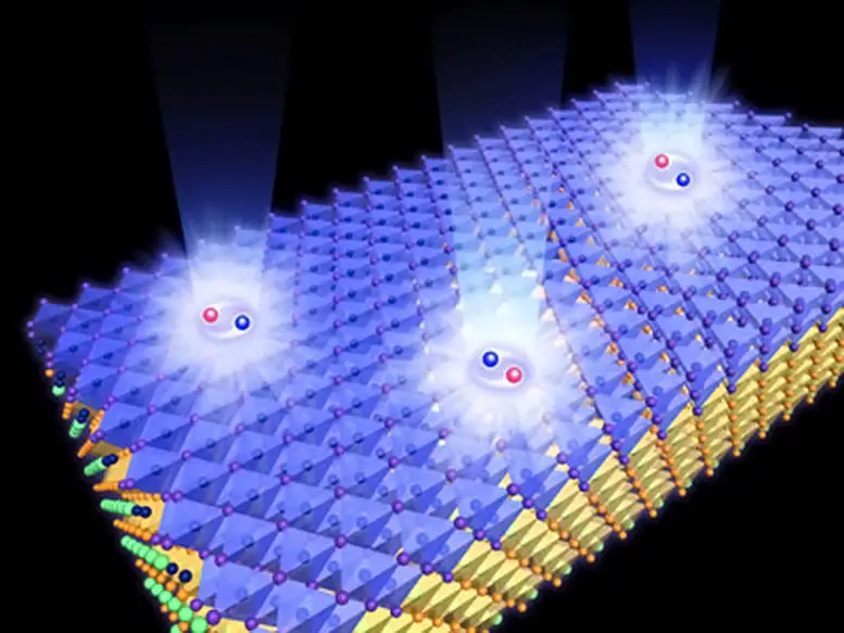
Nakamura and his associates tested the purity using photoluminescence, or light particles, at the material’s surface. These photons are absorbed into the fabric, causing electrons to rise to higher energy states and emitting new photons. The team monitored the light emitted by the crystals and determined that it was a perfect single-crystal film. Nakamura says, “We expected that the quality would improve using our method.” “But the results exceeded all our expectations.”
Nakamura and his group plan to combine semiconductors of different halides and explore new properties. Nakamura says, “We will investigate emerging novel functionalities as well as physics at the interfaces of halide halides.”
Enabling Better Optoelectronic Devices With Thin Cuprous Iodide Film