
The core of optical communication is the conversion of information into light and the transmission of it via optical fibers. Optic fibers made of silica are deficient in a loss at 0.2 dB/km. They have helped build the foundations for today’s global telecommunication networks and our information society.
This ultralow optical loss is also essential for integrated photonics. These enable visual signal processing, detection, and synthesis via on-chip waveguides. Many innovative technologies today are based upon integrated photonics. These include semiconductor lasers and modulators as well as photodetectors. They are widely used in data centers, computing, sensing, computing, and communications.
Most integrated photonic chips are made from abundant silicon with good optical properties. New material platforms have been created to replace silicon. But silicon cannot do all the things we need in integrated photos. Si3N4 is one of these materials. It has a shallow optical loss (or orders of magnitude lower than silicon). It is the preferred material for applications that require low loss, such as narrow-linewidth lasers, photonic delay lines, and nonlinear photos.
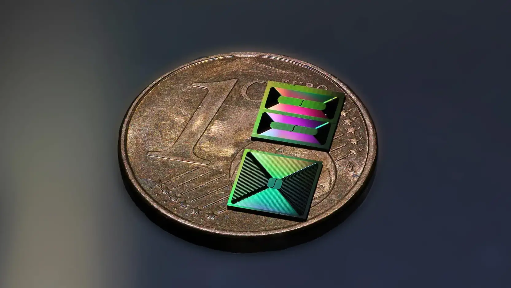
Scientists in Professor Tobias J. Kippenberg’s School of Basic Sciences at EPFL have now developed a new technology to build silicon nitride integrated photonic circuits that are extremely low in optical losses and tiny footprints. The paper is published in Nature Communications.
The technology combines nanofabrication with material science and is based on EPFL’s photonic Damascene process. The team created integrated circuits with optical losses as low as 1 dB/m. This is a record for nonlinear integrated photonic materials. This low loss significantly reduces power requirements for chip-scale optical frequency combines (“micro combs”) that are used in optical atomic clocks, coherent optical transceivers, and low-noise microwave synthesizers. The team used the new technology to create waveguides measuring meters on microresonators with high-quality-factor microresonators and 5x5mm2 chips. The team also reported a high fabrication yield which is crucial for scaling up industrial production,” said Junqiu Liu, who was responsible for the fabrication at EPFL’s Center of MicroNanoTechnology. “We also look forward to our technology being used in emerging applications like coherent LiDAR and photonic neural networks, as well as quantum computing.