
A global research team has made significant progress in developing materials for quantum sensor technology. This technology could benefit medicine, navigation, and IT in the future.
Boron nitride, compatible with other two-dimensional crystal structures, is technologically fascinating. This opens up new possibilities for artificial heterostructures and electronic devices that are based on them.
About a year ago, a team from the Institute of Physics at Julius-Maximilians-Universitat (JMU) Wurzburg in Bavaria, Germany, succeeded in creating spin defects, also known as qubits, in a layered crystal of boron nitride and identifying them in experimentally.
Recent research by the team of Professor Vladimir Dyakonov and his Ph.D. student Andreas Gottschalk, as well as group leader PD Dr. Andreas Sperlich, has led to an essential step in the next phase: the controlled coherent control of spin defects at room temperature. The findings of the researchers were published in the influential journal Science Advances. Despite the pandemic, the research was done closely with Trent University in Canada and the University of Technology Sydney in Australia.
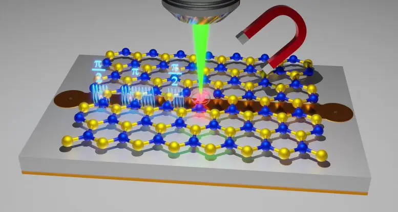
Researchers at JMU plan to create such a stackable structure. It comprises semiconducting molybdenum disulfide (top), metallic graphene, and insulating boron nitride (bottom). The red dot represents the single spin defect within one of the layers of boron-nitride. This defect can be used as a probe within the stack.
Even more precise measurements of local electromagnetic fields
Vladimir Dyakonov explains that materials with spin defects can be controlled to allow for more accurate measurements of the local electromagnetic field. This is because they are at the boundary of the rest of the world, which must be mapped. Imaging in medicine, navigation, and everywhere else where contactless measurement is required of electromagnetic fields are possible application areas.
Andreas Sperlich adds that although the search for the best material is ongoing, many potential candidates exist. We have found a candidate that is unique because of its flat geometry. This allows for the most significant integration possibilities in electronics.
It is difficult to overcome the limitations of spin coherence times.
JMU was the site of all spin-sensitive experiments using boron Nitride. Andreas Gottscholl (Ph.D. student, first author) said that they could determine the limits of spin coherence times and measure them. Knowing spin coherence time is essential to determine the potential spin defects in quantum applications. Long coherence times are desirable for complex manipulations.
Gottscholl summarizes the principle: “Imagine that a gyroscope rotates around its axis. We have shown that these mini gyroscopes can exist in a boron nitride layer. We have now shown how to control the Gyroscope. This means that any angle can deflect it without touching it, and, most importantly, it can be held.
Coherence time reacts sensibly to neighboring atomic layers.
Contactless manipulation of the “gyroscope,” the spin state, was possible using the pulsed, high-frequency electromagnetic field and the resonant microwaves. Researchers at JMU also determined the time it takes for the “Gyroscope to maintain its new orientation. The deflection angle is a simplified illustration that shows how a qubit can take on many states. It doesn’t have to be 0 or 1, as in a bit.
What does all this have to do with sensor technology? The crystal’s atomic environment can affect the manipulated spin state and significantly reduce its coherence time. Andreas Sperlich explains, “We were able to show how sensitive the coherence reacts at a distance to atoms and nuclei. To temperature and magnetic fields. So the qubit’s environment is deduced using the measurement of coherence time.”
Ziel: Electronic devices with spin-decorated boron Nitride layers
Next, the JMU team plans to create an artificially stacked two-dimensional crystal from different materials. This includes a spin-bearing component. The latter’s essential building blocks are atomically thin boron nitride layers containing optically active defects and an accessible spin state.
“It would be very appealing to control spin defects and their surrounding in 2D devices not just optically but also via the electric current.” Vladimir Dyakonov says that this is an entirely new area.